Core technology
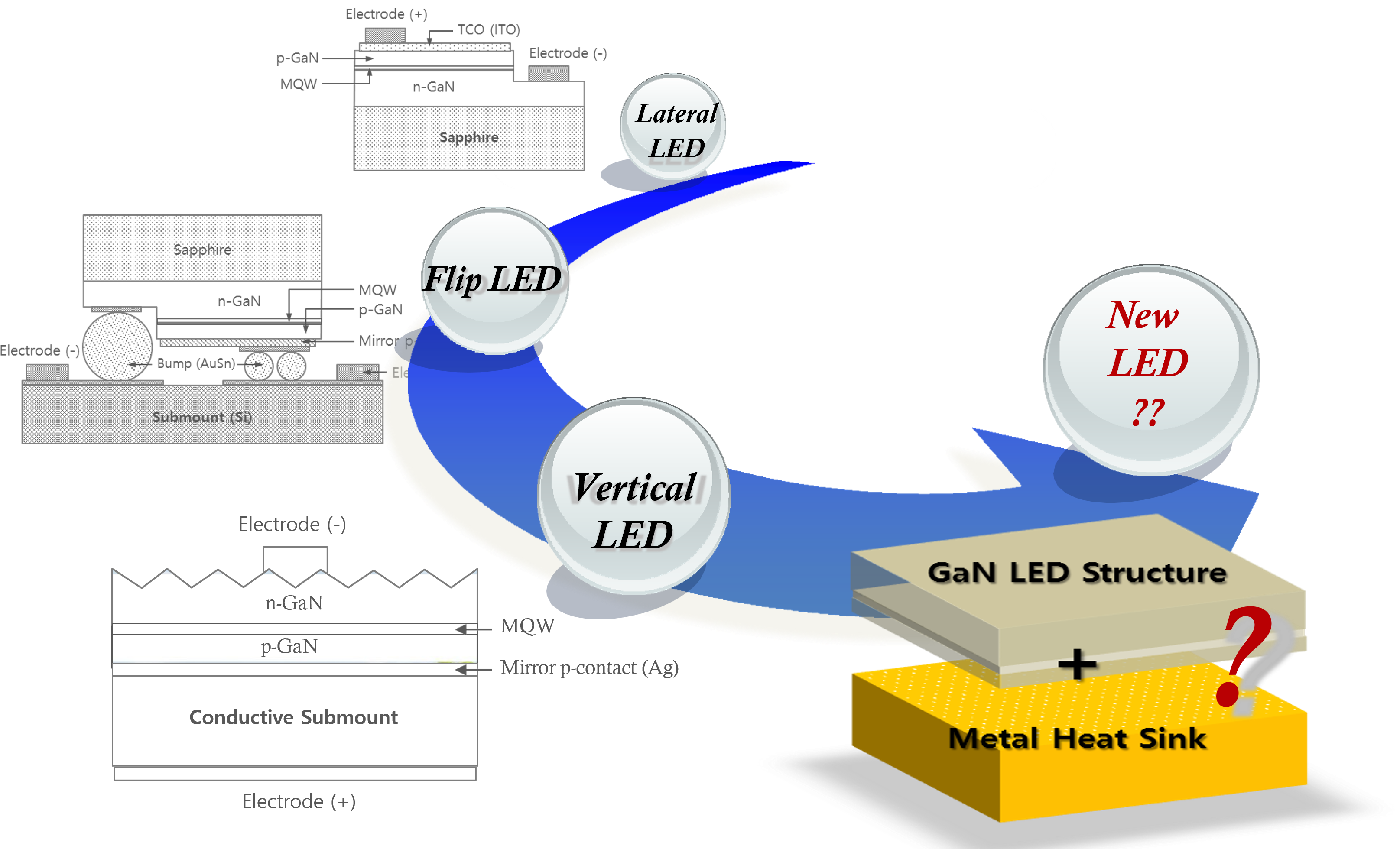
Conventional lateral and vertical structures hit current crowding and thermal limits at high power. The HHP structure changes electrode geometry and substrate material together, solving both at once.
01 — Structure
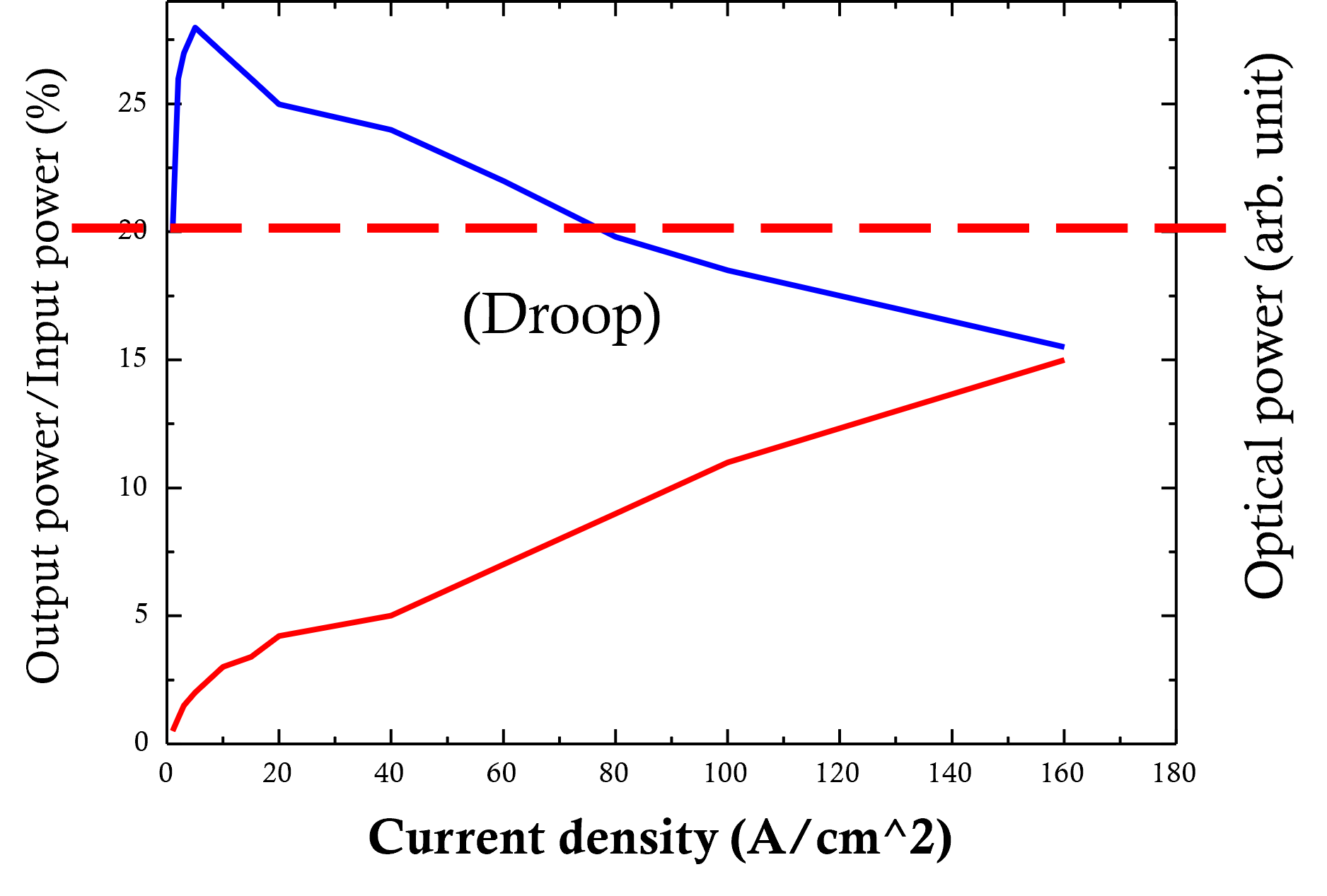
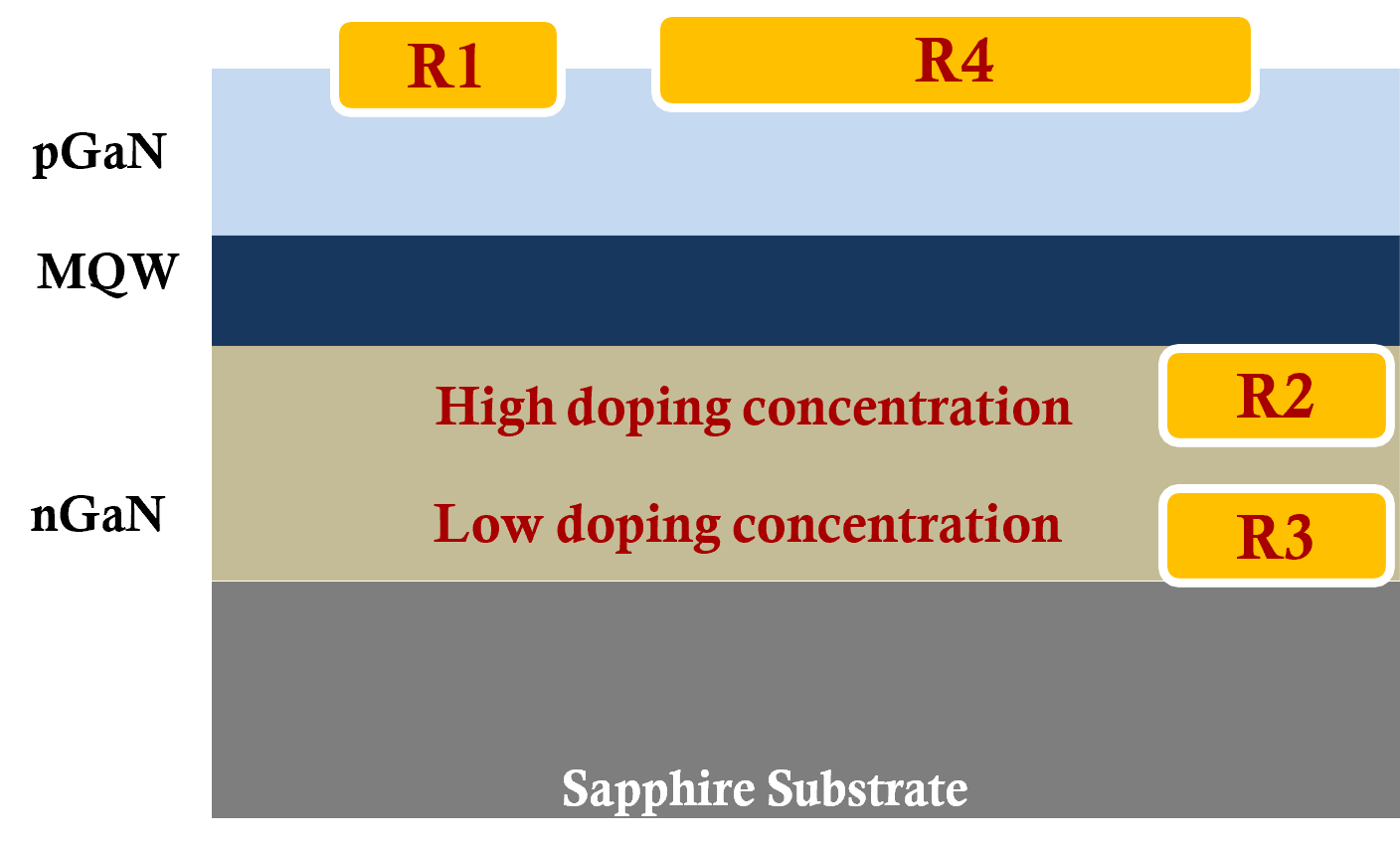
The electrode is formed as a plane on a high-doping-concentration layer rather than a point. Current spreads evenly across the whole chip, so localized current crowding disappears and the forward voltage (Vf) stays low. As a result efficiency (lm/W) does not collapse even at high drive currents, delivering the best current spreading and reliability (★★★) among lateral and vertical structures.
The sapphire beneath the emitting layer is replaced with a plated-copper metal substrate, resolving the fundamental heat problem of sapphire structures. Thermal conductivity rises more than 300% over a conventional lateral structure, so heat does not accumulate and light output is maintained even under high-current drive. Combined with a textured n-GaN surface, it secures a light-emitting area above 90%.
A stable structure that keeps only the strengths of the lateral and vertical types achieves a 95% production yield by lowering process complexity without the vertical type's expensive bonding process. Unlike the conventional lateral structure, which loses competitiveness at high power, it enables high-power mass production and cuts manufacturing cost to about a third of competitors.
| Lateral | Vertical | HHP-LED | |
|---|---|---|---|
| Substrate | Insulating sapphire (Al₂O₃) | Conductive submount | Plated copper (Plated-Cu) |
| Emitting area | Efficiency ~80% | Efficiency >90% · brighter via texturing / PHC extraction | Efficiency >90% · brighter via texturing / PHC extraction |
| Heat dissipation | 100% (ref.) | >300% · maximized by metal substrate | >300% · maximized by metal substrate |
| High-current efficiency | Sharp drop · low-conductivity substrate is the cause | Decline · high-conductivity substrate applied | Suppressed decline · electrode on high-doping layer and ultra-low Vf structure improve lm/W |
| Current spread | ★☆☆ | ★★☆ | ★★★ |
| Remarks | Uncompetitive above 3W | N-face GaN ohmic contact · costly bonding process | Low-cost, high-reliability mass production |
02 — Specifications
Test conditions and reports are included in the datasheet. Competitor figures are from public sources.
03 — COB module
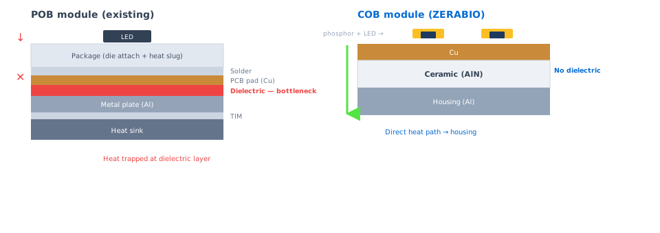
The first 500 W single COB module to be commercialized. A ceramic-based chip-on-board structure secures both heat dissipation and reliability.
04 — Evolution
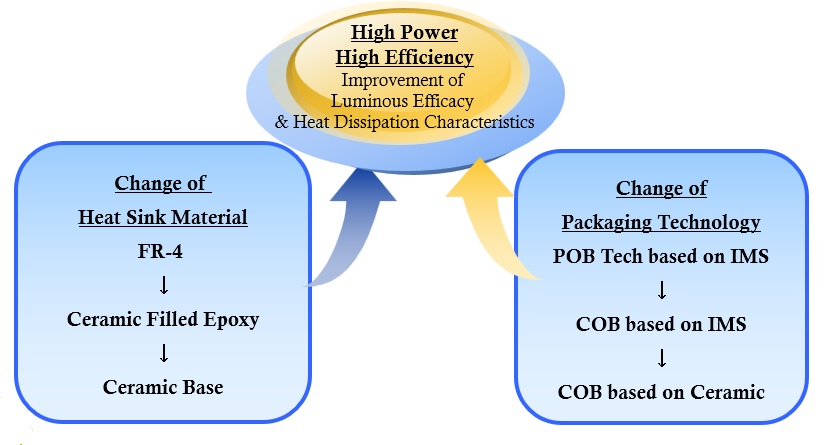
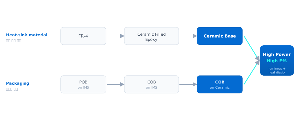
We moved from POB (Package on Board), which welds a lead-frame package onto the board, to COB (Chip on Board), which mounts the bare chip directly. In parallel the heat-sink substrate evolved FR-4 → ceramic-filled epoxy → ceramic base, cutting the part count while achieving high power and high efficiency together.
05 — Measured thermals
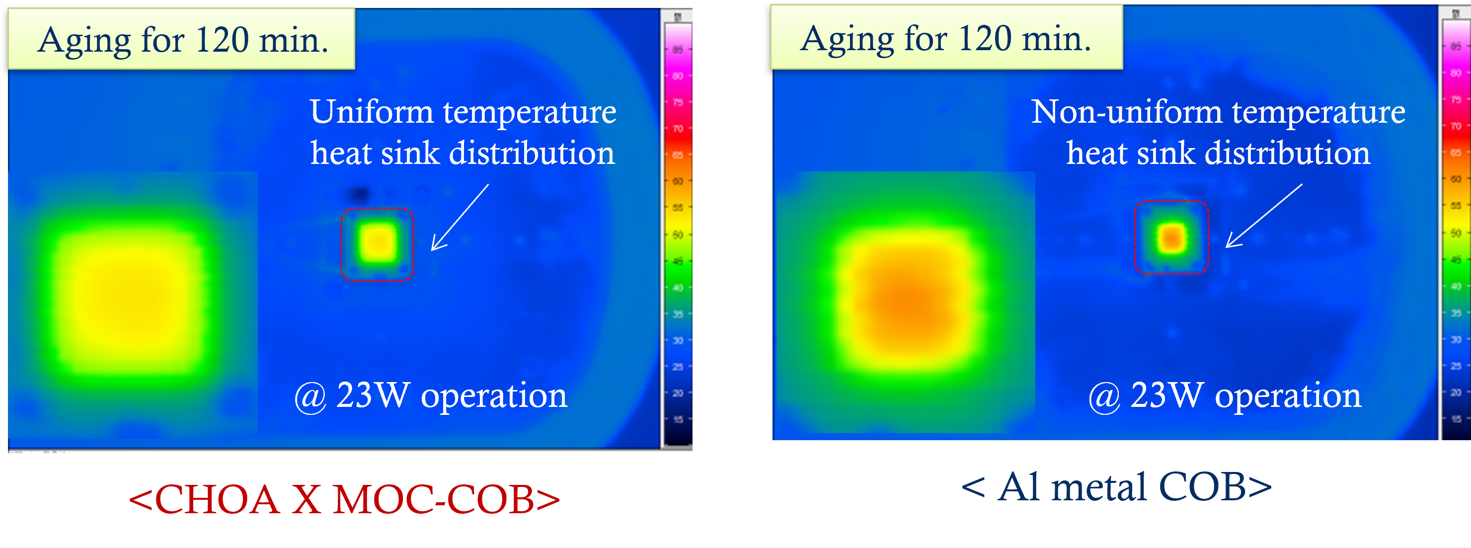
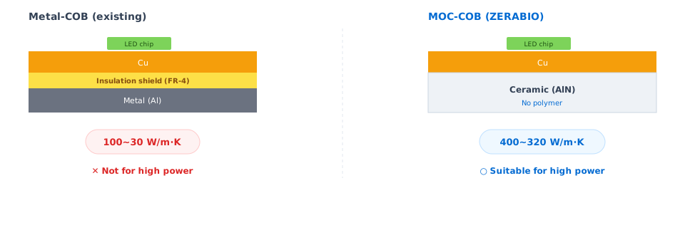
By removing the polymer insulation layer and laminating a highly conductive metal onto ceramic (AlN), MOC-COB reaches a far higher substrate thermal conductivity than a conventional metal COB. Measured under identical 23 W drive over 120 minutes of aging.
| Item | Metal-COB | MOC-COB | Advantage |
|---|---|---|---|
| Substrate conductivity | 100–30 W/m·K | 400–320 W/m·K | No polymer insulation layer |
| LED chip surface temp. | 61.1 ℃ | 53.4 ℃ | 7.7 ℃ lower |
| Thermal resistance (LED→Case) | 1.25 ℃/W | 0.91 ℃/W | 0.35 ℃/W lower |
| Voltage drop | −1.16 % | −0.97 % | 0.19 %p lower |
Conditions · 23 W drive, 120 min aging. Source · ZeraBio test report (III. LED Technology Status).
06 — Ceramic thick film
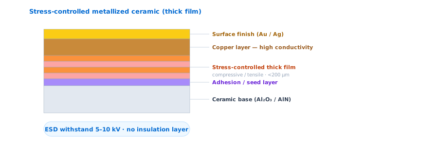
Metal is sputtered onto ceramic as a thick film, with compressive and tensile stress alternated under control so the film thickens without delamination. The key is removing the insulation layer from the heat path.
07 — Competitive edge
Our three core patented technologies, set side by side with the global leaders.
| Technology | ZERABIO | Competitors |
|---|---|---|
| Phosphor formula | Delivers high power (500 W) and high CRI (98 Ra) together, and covers plant grow lights via phosphor spreading | Cree at 95 Ra, most of the market 80–90 Ra · high power relies on RGB/POB with light-uniformity and fixture-size limits |
| MOC-COB | Highly conductive metal laminated on an insulation-free ceramic wiring board — over 10 A allowable current, high-power COB | Cree and Samsung use ceramic but stay around 75 W max due to the insulation shield |
| Horizontal power LED chip | Sapphire heat problem solved — up to 20 W per single chip, mass-produced at 95% yield | Samsung, LG Innotek, Seoul Semiconductor, Cree, Osram cap at 3 W per chip and struggle to mass-produce at low yield |
Chip structure, electrode layout, substrate and thermal design, and module reliability are each protected separately. Working around one leaves the rest.
View the full portfolioSouth Korea
United States
Japan